stm32l151初始化时间(STM32L431时钟系统初始化示例)
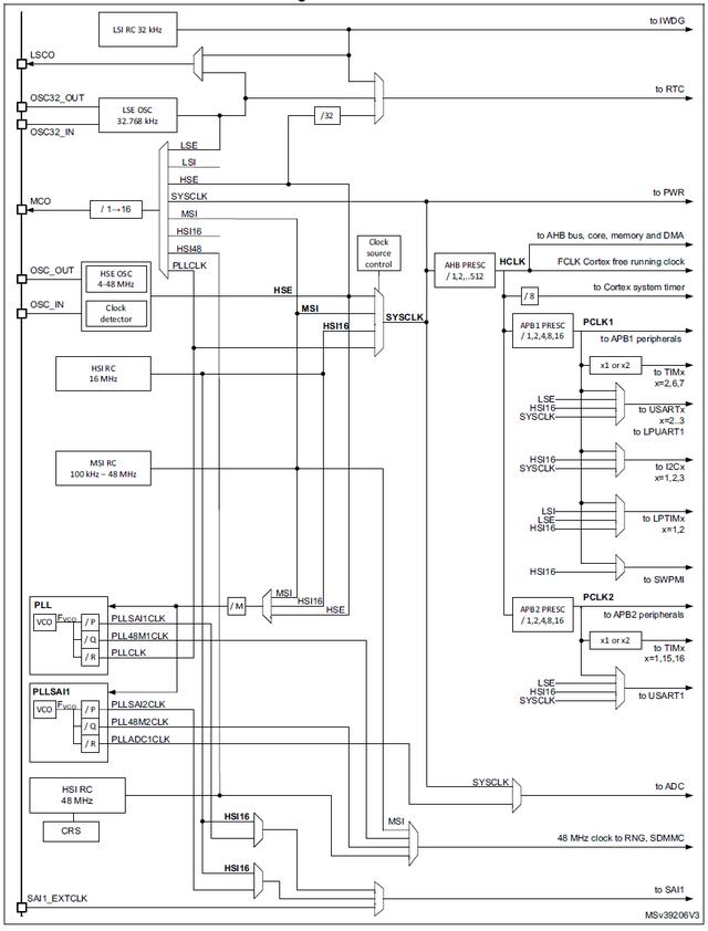
STM32L431有4个时钟源可以作为系统时钟:
- HSE: 高速外部晶体或陶瓷谐振器, 4 MHz - 48 MHz
- HSI16: 高速内部RC振荡器, 16 MHz
- MSI: 多种频率可选的内部RC振荡器, 100KHz - 48MHz 之间共有12档频率可选
- PLL: 系统内部的PLL, 可以将HSE, HSI16, MSI作为输入时钟源, 设置倍频系数, 输出最高80MHz作为系统时钟
系统上电后, 默认MSI(4MHz)作为系统时钟, 但本文将使用HSE(24.576MHz的外部晶振)作为PLL的输入时钟源,使PLL产生73.728MHz作为系统时钟.
下图为STM32L431的时钟系统结构框图:
实现HSE作为PLL时钟源,并将PLL输出作为系统时钟的源程序如下:
typedef struct
{
  __IO uint32_t CR;          /*!< RCC clock control register,                                */
  __IO uint32_t ICSCR;       /*!< RCC Internal Clock Sources Calibration Register,           */
  __IO uint32_t CFGR;        /*!< RCC clock configuration register,                          */
  __IO uint32_t PLLCFGR;     /*!< RCC System PLL configuration register,                     */
  __IO uint32_t PLLSAI1CFGR; /*!< RCC PLL SAI1 Configuration Register,                       */
  uint32_t      RESERVED_0;  /*!< Reserved,                                                  */
  __IO uint32_t CIER;        /*!< RCC Clock Interrupt Enable Register,                       */
  __IO uint32_t CIFR;        /*!< RCC Clock Interrupt Flag Register,                         */
  __IO uint32_t CICR;        /*!< RCC Clock Interrupt Clear Register,                        */
  uint32_t      RESERVED0;   /*!< Reserved,                                                  */
  __IO uint32_t AHB1RSTR;    /*!< RCC AHB1 peripheral reset register,                        */
  __IO uint32_t AHB2RSTR;    /*!< RCC AHB2 peripheral reset register,                        */
  __IO uint32_t AHB3RSTR;    /*!< RCC AHB3 peripheral reset register,                        */
  uint32_t      RESERVED1;   /*!< Reserved,                                                  */
  __IO uint32_t APB1RSTR1;   /*!< RCC APB1 macrocells resets Low Word,                       */
  __IO uint32_t APB1RSTR2;   /*!< RCC APB1 macrocells resets High Word,                      */
  __IO uint32_t APB2RSTR;    /*!< RCC APB2 macrocells resets,                                */
  uint32_t      RESERVED2;   /*!< Reserved,                                                  */
  __IO uint32_t AHB1ENR;     /*!< RCC AHB1 peripheral clock enable register,                 */
  __IO uint32_t AHB2ENR;     /*!< RCC AHB2 peripheral clock enable register,                 */
  __IO uint32_t AHB3ENR;     /*!< RCC AHB3 peripheral clock enable register,                 */
  uint32_t      RESERVED3;   /*!< Reserved,                                                  */
  __IO uint32_t APB1ENR1;    /*!< RCC APB1 macrocells clock enables Low Word,                */
  __IO uint32_t APB1ENR2;    /*!< RCC APB1 macrocells clock enables High Word,               */
  __IO uint32_t APB2ENR;     /*!< RCC APB2 macrocells clock enabled,                         */
  uint32_t      RESERVED4;   /*!< Reserved,                                                  */
  __IO uint32_t AHB1SMENR;   /*!< RCC AHB1 macrocells clocks enables in sleep mode,          */
  __IO uint32_t AHB2SMENR;   /*!< RCC AHB2 macrocells clock enables in sleep mode,           */
  __IO uint32_t AHB3SMENR;   /*!< RCC AHB3 macrocells clock enables in sleep mode,           */
  uint32_t      RESERVED5;   /*!< Reserved,                                                  */
  __IO uint32_t APB1SMENR1;  /*!< RCC APB1 macrocells clock enables in sleep mode Low Word,  */
  __IO uint32_t APB1SMENR2;  /*!< RCC APB1 macrocells clock enables in sleep mode High Word, */
  __IO uint32_t APB2SMENR;   /*!< RCC APB2 macrocells clock enabled in sleep mode,           */
  uint32_t      RESERVED6;   /*!< Reserved,                                                  */
  __IO uint32_t CCIPR;       /*!< RCC IPs Clocks Configuration Register,                     */
  __IO uint32_t RESERVED7;   /*!< Reserved,                                                  */
  __IO uint32_t BDCR;        /*!< RCC Vswitch Backup Domain Control Register,                */
  __IO uint32_t CSR;         /*!< RCC clock control & status register,                       */
  __IO uint32_t CRRCR;       /*!< RCC Clock recovery RC register,                            */
  __IO uint32_t CCIPR2;      /*!< RCC Peripherals independent clock configuration register,  */
} RCC_TypeDef;

#define PERIPH_BASE       ((uint32_t)0x40000000)
#define AHB1PERIPH_BASE   (PERIPH_BASE   0x00020000)
#define RCC_BASE          (AHB1PERIPH_BASE   0x1000)
#define RCC               ((RCC_TypeDef *) RCC_BASE)

#define  RCC_CR_HSEON     ((uint32_t)0x00010000)
#define  RCC_CR_HSERDY    ((uint32_t)0x00020000)
#define  RCC_CR_PLLON     ((uint32_t)0x01000000)
#define  RCC_CR_PLLRDY    ((uint32_t)0x02000000)

#define  RCC_PLLCFGR_PLLSRC_HSE    ((uint32_t)0x00000003)
#define  RCC_PLLCFGR_PLLREN        ((uint32_t)0x01000000)

#define  RCC_CFGR_HPRE_DIV1        ((uint32_t)0x00000000)
#define  RCC_CFGR_PPRE1_DIV4       ((uint32_t)0x00000500)
#define  RCC_CFGR_PPRE2_DIV4       ((uint32_t)0x00002800)
#define  RCC_CFGR_SW_PLL           ((uint32_t)0x00000003)

#define  RCC_CFGR_SWS              ((uint32_t)0x0000000C)
#define  RCC_CFGR_SWS_PLL          ((uint32_t)0x0000000C)

/*
* 初始化STM32L431时钟系统
*
* 输入时钟: HSE(24.576MHz)
*
* PLL输出:  73.728MHz
*/
void RCC_Init(void)
{
    /*****************************************
    * 1. 启动HSE
    ******************************************/

    // MSI = 4MHz, MSI时钟开
    RCC->CR = 0x00000063;

    // HSE时钟开
    RCC->CR |= RCC_CR_HSEON;

    // 等待HSE工作正常
    for(;;)
    {
        if (RCC->CR & RCC_CR_HSERDY) break;
    }


    /*****************************************
    * 2. 启动PLL
    ******************************************/

    // 此寄存器设置了: PLLN = 12 , PLLM = 2 , PLLR = 2
    RCC->PLLCFGR = 0x00000C10;

    // 将HSE(24.576M)指定为PLL的时钟源, PLLSRC = 24.576MHz
    RCC->PLLCFGR |= RCC_PLLCFGR_PLLSRC_HSE;

    // fVCO = PLLSRC * (PLLN / PLLM) = 24.576M * (12 / 2) = 147.456M
    // PLLCLK = fVCO / PLLR = fVCO / 2 = 73.728M

    // PLL开
    RCC->CR |= RCC_CR_PLLON;

    // 等待PLL工作正常
    for(;;)
    {
        if (RCC->CR & RCC_CR_PLLRDY) break;
    }

    // PLLCLK输出允许
    RCC->PLLCFGR |= RCC_PLLCFGR_PLLREN;


    /*****************************************
    * 3. 分配各时钟频率
    ******************************************/

    RCC->CFGR  = 0;

    // AHB -HCLK  = SYSCLK / 1 = 73.728MHz
    RCC->CFGR |= RCC_CFGR_HPRE_DIV1;

    // APB1-PCLK1 = HCLK   / 4 = 18.432MHz
    RCC->CFGR |= RCC_CFGR_PPRE1_DIV4;

    // APB2-PCLK2 = HCLK   / 4 = 18.432MHz
    RCC->CFGR |= RCC_CFGR_PPRE2_DIV4;


    // 选择 PLLCLK(73.728MHz) 作为SYSCLK
    RCC->CFGR |= RCC_CFGR_SW_PLL;

    // 等待SYSCLK = PLLCLK选择成功
    for(;;)
    {
        if ((RCC->CFGR & RCC_CFGR_SWS) == RCC_CFGR_SWS_PLL) break;
    }
}
免责声明:本文仅代表文章作者的个人观点,与本站无关。其原创性、真实性以及文中陈述文字和内容未经本站证实,对本文以及其中全部或者部分内容文字的真实性、完整性和原创性本站不作任何保证或承诺,请读者仅作参考,并自行核实相关内容。文章投诉邮箱:anhduc.ph@yahoo.com


